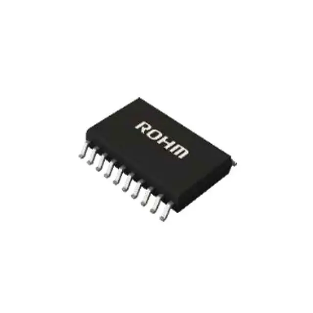
Images are for reference only
SN74ACT244DW
IC BUF NON-INVERT 5.5V 20SOIC
- Manufacturer
- Mfr. Part #SN74ACT244DW
- Package SOIC-20
- Datasheet
- In Stock2836
100% Original & New
24 Hours ready to ship
365 Days Warranty
RFQ & Get more Discounts
Specifications
| Package | Bulk,Tube |
| Series | 74ACT |
| ProductStatus | Active |
| LogicType | Buffer, Non-Inverting |
| NumberofElements | 2 |
| NumberofBitsperElement | 4 |
| OutputType | 3-State |
| Current-OutputHighLow | 24mA, 24mA |
| Voltage-Supply | 4.5V ~ 5.5V |
| OperatingTemperature | -40°C ~ 85°C (TA) |
| MountingType | Surface Mount |
| Package/Case | 20-SOIC (0.295, 7.50mm Width) |
Overview
Description
This integrated circuit is particularly beneficial for driving capacitive loads and enhancing signal integrity over long distances. The device has a tri-state output, allowing multiple outputs to be connected to a single bus without signal contention. Its fast propagation delay and low output skew make it suitable for high-frequency applications.
The SN74ACT244DW is packaged in a surface-mount 20-pin TSSOP, which minimizes board space and facilitates efficient thermal management. It is commonly used in data buffering, signal routing, and interfacing applications in various electronic systems, including computers, communication devices, and consumer electronics.
Features
1. Logic Levels: Compatible with both TTL and CMOS logic levels.
2. High-Speed Operation: Typical propagation delay of 7 ns (max at 25°C).
3. Output Drive: Capable of driving up to 64 mA on outputs, suitable for driving heavy loads.
4. Tri-State Outputs: Each output can be enabled or disabled, allowing for bus-oriented applications.
5. Wide Supply Voltage: Operates from 4.5V to 5.5V, ensuring flexibility in design.
6. Low Power Consumption: Designed to consume minimal power during operation.
7. Temperature Range: Rated for operation from -40°C to 125°C.
8. Pin Configuration: Available in a 20-pin TSSOP package for compact designs.
These features make the SN74ACT244DW ideal for applications requiring signal buffering and driving capabilities, such as in data communication and digital interfacing.
Package
Pinout
Pin Count and Function:
- Pins 1-8: These are the data input pins (A1 to A8).
- Pins 9-16: These are the corresponding output pins (Y1 to Y8).
- Pin 19 (GND): Ground connection.
- Pin 20 (VCC): Power supply connection.
- Pin 17 (OE): Output enable control pin; active low. When OE is low, the outputs are enabled, and when high, they are in a high-impedance state.
- Pin 18 (DIR): Direction control pin; it determines the data flow direction.
The device operates with a supply voltage range of 4.5V to 5.5V and offers improved speed and drive capability compared to traditional TTL buffers.
Manufacturer
Application
Equivalent
Shipping
Shipping MethodsWe
offer global shipping services through DHL, FedEx, TNT, UPS, or any other forwarder of your choice.
Shipping Fee Reference (DHL/FedEx):
DHL: Shipping cost ranges from $25-$45 (0.5kg), with an estimated delivery time of 2-5 business days.
FedEx: Shipping cost ranges from $25-$40 (0.5kg), with an estimated delivery time of 3-7 business days.
UPS: Shipping cost ranges from $25-$45 (0.5kg), with an estimated delivery time of 3-7 business days.
TNT: Shipping cost ranges from $25-$65 (0.5kg), with an estimated delivery time of 3-7 business days.
EMS: Shipping cost ranges from $30-$50 (0.5kg), with an estimated delivery time of 7-15 business days.
Registered Air Mail: Shipping cost is $2-$4 (0.1kg), with an estimated delivery time of 5-20 business days.
Payments
Payment Methods
The Payment term is 100% Prepaid.
Currently, we only accept the below payment methods:
1. PayPal
2. Credit/ Debit Card
3. Wire Transfer
Similar
-
![MX25L3233FZBI-08Q]() MX25L3233FZBI-08Q
Macronix
-
![MX25V1635FZNI]() MX25V1635FZNI
Macronix
-
![MX29F400CBTI-70G]() MX29F400CBTI-70G
Macronix
-
![MX66U1G45GXDI00]() MX66U1G45GXDI00
Macronix
-
![MX25V2033FM1I]() MX25V2033FM1I
Macronix
-
![MX25R3235FZNIL0]() MX25R3235FZNIL0
Macronix
-
![MX25L25673GMI-10G]() MX25L25673GMI-10G
Macronix
-
![MX25L2006EM1I-12G]() MX25L2006EM1I-12G
Macronix
-
![MX25R1635FZUIH0]() MX25R1635FZUIH0
Macronix
-
![MX25L6433FM2I-08G]() MX25L6433FM2I-08G
Macronix
-
![MX29F040CQI-70G]() MX29F040CQI-70G
Macronix
-
![MX29F800CBTI-70G]() MX29F800CBTI-70G
Macronix