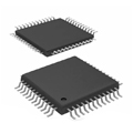
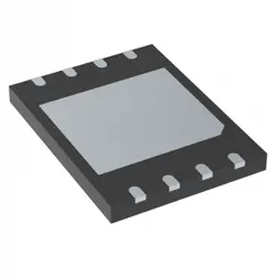
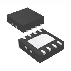
Images are for reference only
STBP112CVDJ6F
IC OVP PROTECTION TDFN-8
- Manufacturer
- Mfr. Part #STBP112CVDJ6F
- Package TDFN-8
- Datasheet STBP112CVDJ6F DataSheet
- In Stock4597
100% Original & New
24 Hours ready to ship
365 Days Warranty
RFQ & Get more Discounts
Specifications
| Package | Tape & Reel (TR),Cut Tape (CT) |
| ProductStatus | Active |
| Technology | Internal Switch |
| NumberofCircuits | 1 |
| Applications | General Purpose |
| MountingType | Surface Mount |
| Package/Case | 8-WFDFN Exposed Pad |
Overview
Description
To provide a precise introduction, it is essential to consult the manufacturer's datasheet or relevant technical documentation, which will detail its specifications, pin configuration, functionalities, applications, and electrical characteristics. If you're looking for more specific information or context regarding STBP112CVDJ6F, please provide more details or clarify the type of component you are interested in.
Features
1. Dual High-Side Switches: It integrates two independent switches, allowing for flexible load management.
2. Low On-Resistance: Offers a low on-resistance (typically around 30 mΩ), which minimizes power loss and heat generation.
3. Wide Supply Voltage Range: Operates within a range of 1.8V to 5.5V, accommodating various applications.
4. Fast Switching Times: Ensures quick response times for efficient operation.
5. Thermal and Overcurrent Protection: Includes features for enhanced reliability, protecting against overheating and overcurrent conditions.
6. Small Package Size: Available in a compact package (SOT-23), making it suitable for space-constrained applications.
7. Low Quiescent Current: Consumes minimal power in standby mode, enhancing energy efficiency.
These features make the STBP112CVDJ6F ideal for applications in portable devices, battery-powered equipment, and general power management.
Package
Pinout
The pin count is 16, with the following key functions:
1. IN_A, IN_B (Pins 1, 2): Input signals for channel A and B to control the MOSFETs.
2. OUT_A, OUT_B (Pins 3, 4): Output signals to drive the gates of the respective MOSFETs.
3. VSUP (Pin 5): Supply voltage input.
4. GND (Pin 6): Ground connection.
5. BOOT_A, BOOT_B (Pins 7, 8): Bootstrap capacitors for high-side MOSFET driving.
6. COMP_A, COMP_B (Pins 9, 10): Compensation pins for stability.
7. R_T (Pin 11): Timing resistor for adjustable delay.
8. VREG (Pin 12): Regulated output voltage for internal circuitry.
9. NC (Pins 13, 14, 15, 16): Not connected pins, typically used for thermal dissipation or reserved for future use.
This device is commonly used in applications like motor control, power management, and DC-DC converters.
Manufacturer
Application
Equivalent
Shipping
Shipping MethodsWe
offer global shipping services through DHL, FedEx, TNT, UPS, or any other forwarder of your choice.
Shipping Fee Reference (DHL/FedEx):
DHL: Shipping cost ranges from $25-$45 (0.5kg), with an estimated delivery time of 2-5 business days.
FedEx: Shipping cost ranges from $25-$40 (0.5kg), with an estimated delivery time of 3-7 business days.
UPS: Shipping cost ranges from $25-$45 (0.5kg), with an estimated delivery time of 3-7 business days.
TNT: Shipping cost ranges from $25-$65 (0.5kg), with an estimated delivery time of 3-7 business days.
EMS: Shipping cost ranges from $30-$50 (0.5kg), with an estimated delivery time of 7-15 business days.
Registered Air Mail: Shipping cost is $2-$4 (0.1kg), with an estimated delivery time of 5-20 business days.
Payments
Payment Methods
The Payment term is 100% Prepaid.
Currently, we only accept the below payment methods:
1. PayPal
2. Credit/ Debit Card
3. Wire Transfer
Similar
-
![MX25V2033FM1I]() MX25V2033FM1I
Macronix
-
![MX25L8035EM2I-10G]() MX25L8035EM2I-10G
Macronix
-
![MX25R6435FBDIL0]() MX25R6435FBDIL0
Macronix
-
![MX25L2006EM1I-12G]() MX25L2006EM1I-12G
Macronix
-
![MX25L12833FZ2I-10G]() MX25L12833FZ2I-10..
Macronix
-
![MX25U25645GXDI00]() MX25U25645GXDI00
Macronix
-
![MX25L12835FZ2I-10G]() MX25L12835FZ2I-10..
Macronix
-
![MX29F040CQI-70G]() MX29F040CQI-70G
Macronix
-
![MX29F800CBTI-70G]() MX29F800CBTI-70G
Macronix
-
![MX25U51245GZ4I00]() MX25U51245GZ4I00
Macronix
-
![MX25L1006EMI-10G]() MX25L1006EMI-10G
Macronix
-
![MX25L4006EM2I-12G]() MX25L4006EM2I-12G
Macronix