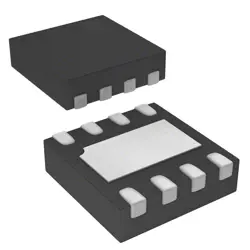
Images are for reference only
TLV271CDBVR
- Manufacturer
- Mfr. Part #TLV271CDBVR
- Package
- Datasheet
- In Stock2775
100% Original & New
24 Hours ready to ship
365 Days Warranty
RFQ & Get more Discounts
Specifications
| Package | Tape & Reel (TR),Cut Tape (CT),Bulk |
| ProductStatus | Active |
| AmplifierType | CMOS |
| NumberofCircuits | 1 |
| OutputType | Rail-to-Rail |
| SlewRate | 2.6V/µs |
| GainBandwidthProduct | 3 MHz |
| Current-InputBias | 1 pA |
| Voltage-InputOffset | 500 µV |
| Current-Supply | 625µA |
| Current-Output/Channel | 8 mA |
| Voltage-SupplySpan(Min) | 2.7 V |
| Voltage-SupplySpan(Max) | 16 V |
| OperatingTemperature | 0°C ~ 70°C |
| MountingType | Surface Mount |
| Package/Case | SC-74A, SOT-753 |
Overview
Description
Key characteristics of the TLV271CDBVR include a low input bias current, low offset voltage, and rail-to-rail output swing, which enhances performance in single-supply and low-voltage operations. It has a bandwidth of approximately 1 MHz and a slew rate of 1 V/µs, making it suitable for applications like sensor interfacing, signal conditioning, portable devices, and battery-powered systems.
The op-amp is known for its low power consumption, with a quiescent current of about 550 µA typical, making it ideal for energy-efficient designs. Its rugged design and high reliability make it a popular choice in both industrial and consumer electronics.
Features
The TLV271CDBVR comes in a small SOT-23 package, which is ideal for space-constrained applications. It is well-suited for use in portable electronics, sensor applications, and other low-power analog applications. Additionally, it operates over a wide temperature range, typically from -40°C to 125°C, making it robust for various environmental conditions.
Package
Pinout
1. Pin 1 (OUT): This is the output pin through which the amplified signal exits the op-amp.
2. Pin 2 (IN- or V- or INverting input): This is the inverting input pin where an input signal is applied. The voltage at this pin is compared with the non-inverting input.
3. Pin 3 (IN+ or V+ or Non-inverting input): This is the non-inverting input pin. The voltage applied here is directly amplified by the op-amp.
4. Pin 4 (V- or GND): This is the negative power supply or ground pin.
5. Pin 5 (V+ or VCC): This is the positive power supply pin.
The TLV271 is designed for low voltage and low power consumption, suitable for battery-powered applications.
Manufacturer
Application
Equivalent
Shipping
Shipping MethodsWe
offer global shipping services through DHL, FedEx, TNT, UPS, or any other forwarder of your choice.
Shipping Fee Reference (DHL/FedEx):
DHL: Shipping cost ranges from $25-$45 (0.5kg), with an estimated delivery time of 2-5 business days.
FedEx: Shipping cost ranges from $25-$40 (0.5kg), with an estimated delivery time of 3-7 business days.
UPS: Shipping cost ranges from $25-$45 (0.5kg), with an estimated delivery time of 3-7 business days.
TNT: Shipping cost ranges from $25-$65 (0.5kg), with an estimated delivery time of 3-7 business days.
EMS: Shipping cost ranges from $30-$50 (0.5kg), with an estimated delivery time of 7-15 business days.
Registered Air Mail: Shipping cost is $2-$4 (0.1kg), with an estimated delivery time of 5-20 business days.
Payments
Payment Methods
The Payment term is 100% Prepaid.
Currently, we only accept the below payment methods:
1. PayPal
2. Credit/ Debit Card
3. Wire Transfer
Similar
-
![MX25L3233FZBI-08Q]() MX25L3233FZBI-08Q
Macronix
-
![MX25L3233FM1I-08Q]() MX25L3233FM1I-08Q
Macronix
-
![MX25V1635FZNI]() MX25V1635FZNI
Macronix
-
![MX29F400CBTI-70G]() MX29F400CBTI-70G
Macronix
-
![MX66U1G45GXDI00]() MX66U1G45GXDI00
Macronix
-
![MX25V16066M1I02]() MX25V16066M1I02
Macronix
-
![MX25V16066M2I02]() MX25V16066M2I02
Macronix
-
![MX30LF2G28AD-TI]() MX30LF2G28AD-TI
Macronix
-
![MX25L8035EM2I-10G]() MX25L8035EM2I-10G
Macronix
-
![MX25L25673GMI-08G]() MX25L25673GMI-08G
Macronix
-
![MX25U25643GZNI00]() MX25U25643GZNI00
Macronix
-
![MX25R1635FZUIH0]() MX25R1635FZUIH0
Macronix