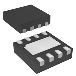
Images are for reference only
TPS61252DSGR
IC BOOST CONV ADJ 1.5A 8WSON
- Manufacturer
- Mfr. Part #TPS61252DSGR
- Package WSON-8
- Datasheet
- In Stock3240
100% Original & New
24 Hours ready to ship
365 Days Warranty
RFQ & Get more Discounts
Specifications
| Package | Tape & Reel (TR),Cut Tape (CT),Bulk |
| ProductStatus | Active |
| Applications | PDA's, Portable Audio/Video, Smartphones |
| Voltage-Supply | 2.3V ~ 6V |
| OperatingTemperature | -40°C ~ 85°C |
| MountingType | Surface Mount |
| Package/Case | 8-WFDFN Exposed Pad |
Overview
Description
It features a low quiescent current, contributing to longer battery life in portable applications. The device operates with high efficiency over a broad load range, thanks to its pulse-width modulation (PWM) and pulse-frequency modulation (PFM) modes. The TPS61252DSGR also includes overcurrent, overtemperature, and short-circuit protection to ensure reliable operation.
Packaged in a small 10-pin VSON (DSG) package, the TPS61252DSGR is suitable for compact designs. Its ease of use, combined with the ability to maintain efficiency across varying loads, makes it a versatile choice for designers seeking a robust boost converter solution in power-sensitive applications.
Features
It also includes power-save mode operation for light-load conditions, reducing power consumption and extending battery life. The TPS61252DSGR features an adjustable output voltage via external resistors, along with an integrated soft-start function to reduce inrush current. For safety, it offers over-current protection, short-circuit protection, and thermal shutdown. The package type is a 10-pin VSON, which allows for compact designs. This boost converter is ideal for portable and battery-powered applications where space and efficiency are critical.
Package
Pinout
Key features of the TPS61252 include:
1. High efficiency for longer battery life.
2. Integrated power MOSFETs for reduced component count and compact design.
3. Adjustable output voltage via an external resistor divider.
4. Overcurrent protection and thermal shutdown for reliability.
The pin configuration typically includes connections for input voltage (VIN), output voltage (VOUT), ground (GND), feedback (FB) for setting output voltage, and control pins such as enable (EN) and power good (PG). Ensure to refer to the datasheet for exact pin functions and layout to avoid errors in circuit design.
Manufacturer
Application
Equivalent
1. LTC3122 from Analog Devices
2. MAX1771 from Maxim Integrated
3. NCP1403 from ON Semiconductor
4. RT4810 from Richtek
These alternatives offer similar functionality in boosting input voltages to higher levels, but it's important to compare their specific features and specifications to ensure compatibility with your application.
Shipping
Shipping MethodsWe
offer global shipping services through DHL, FedEx, TNT, UPS, or any other forwarder of your choice.
Shipping Fee Reference (DHL/FedEx):
DHL: Shipping cost ranges from $25-$45 (0.5kg), with an estimated delivery time of 2-5 business days.
FedEx: Shipping cost ranges from $25-$40 (0.5kg), with an estimated delivery time of 3-7 business days.
UPS: Shipping cost ranges from $25-$45 (0.5kg), with an estimated delivery time of 3-7 business days.
TNT: Shipping cost ranges from $25-$65 (0.5kg), with an estimated delivery time of 3-7 business days.
EMS: Shipping cost ranges from $30-$50 (0.5kg), with an estimated delivery time of 7-15 business days.
Registered Air Mail: Shipping cost is $2-$4 (0.1kg), with an estimated delivery time of 5-20 business days.
Payments
Payment Methods
The Payment term is 100% Prepaid.
Currently, we only accept the below payment methods:
1. PayPal
2. Credit/ Debit Card
3. Wire Transfer
Similar
-
![MX25L3233FM1I-08Q]() MX25L3233FM1I-08Q
MX25L3233FM1I-08Q
Macronix
-
![MX25V1635FZNI]() MX25V1635FZNI
MX25V1635FZNI
Macronix
-
![MX29F400CBTI-70G]() MX29F400CBTI-70G
MX29F400CBTI-70G
Macronix
-
![MX66U1G45GXDI00]() MX66U1G45GXDI00
MX66U1G45GXDI00
Macronix
-
![MX25V2033FM1I]() MX25V2033FM1I
MX25V2033FM1I
Macronix
-
![MX25L8035EM2I-10G]() MX25L8035EM2I-10G
MX25L8035EM2I-10G
Macronix
-
![MX25L25673GMI-10G]() MX25L25673GMI-10G
MX25L25673GMI-10G
Macronix
-
![MX25U51279GXDR00]() MX25U51279GXDR00
MX25U51279GXDR00
Macronix
-
![MX25V1635FM2I]() MX25V1635FM2I
MX25V1635FM2I
Macronix
-
![MX25U3232FZBI02]() MX25U3232FZBI02
MX25U3232FZBI02
Macronix
-
![MX25L12833FZ2I-10G]() MX25L12833FZ2I-10..
MX25L12833FZ2I-10..
Macronix
-
![MX29F040CTI-70G]() MX29F040CTI-70G
MX29F040CTI-70G
Macronix