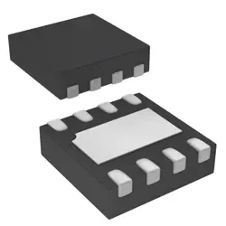
Images are for reference only
W29N02GZBIBF
IC FLASH 2GBIT PARALLEL 63VFBGA
- Manufacturer
- Mfr. Part #W29N02GZBIBF
- Package
- Datasheet
- In Stock4314
100% Original & New
24 Hours ready to ship
365 Days Warranty
RFQ & Get more Discounts
Specifications
| Series | SpiFlash® |
| Part Status | Active |
| Memory Type | Non-Volatile |
| Memory Format | FLASH |
| Technology | FLASH - NAND (SLC) |
| Memory Size | 2Gbit |
| Memory Organization | 256M x 8 |
| Memory Interface | Parallel |
| Write Cycle Time - Word, Page | 35ns |
| Voltage - Supply | 1.7V ~ 1.95V |
| Operating Temperature | -40°C ~ 85°C (TA) |
| Mounting Type | Surface Mount |
| Package / Case | 63-VFBGA |
| Supplier Device Package | 63-VFBGA (9x11) |
| Access Time | 25 ns |
Overview
Description
Features
1. Storage Capacity: It typically denotes the storage size, e.g., 2GB, 4GB, etc.
2. Technology Type: Could be NAND or NOR flash memory, determining how data is accessed and stored.
3. Voltage: Indicates operating voltage, e.g., 1.8V, 3.3V.
4. Package Type: Refers to the physical casing and connection interface, e.g., BGA, TSOP.
5. Read/Write Speed: Defines how fast data can be read from or written to the chip.
6. Operating Temperature: Specifies temperature range for reliable operation.
7. Endurance and Retention: Number of write/erase cycles and data retention period.
8. Security Features: May include encryption support or protection against unauthorized access.
For precise details, it’s best to consult the manufacturer's datasheet or product documentation.
Package
Pinout
Pin Count:
- 48 pins
Key Functions and Pin Descriptions:
- I/O Pins (I/O 0–7): Used for data input and output.
- CLE (Command Latch Enable): Enables command input to the data register.
- ALE (Address Latch Enable): Enables address input to the data register.
- CE# (Chip Enable): Activates the chip for operation.
- WE# (Write Enable): Controls data writing to the device.
- RE# (Read Enable): Controls data reading from the device.
- WP# (Write Protect): Protects data from being written or erased.
- R/B# (Ready/Busy): Indicates device status.
- VCC: Power supply.
- VSS: Ground.
These pins work together to perform standard NAND Flash operations such as reading, writing, and erasing data.
Manufacturer
Application
Equivalent
Shipping
Shipping MethodsWe
offer global shipping services through DHL, FedEx, TNT, UPS, or any other forwarder of your choice.
Shipping Fee Reference (DHL/FedEx):
DHL: Shipping cost ranges from $25-$45 (0.5kg), with an estimated delivery time of 2-5 business days.
FedEx: Shipping cost ranges from $25-$40 (0.5kg), with an estimated delivery time of 3-7 business days.
UPS: Shipping cost ranges from $25-$45 (0.5kg), with an estimated delivery time of 3-7 business days.
TNT: Shipping cost ranges from $25-$65 (0.5kg), with an estimated delivery time of 3-7 business days.
EMS: Shipping cost ranges from $30-$50 (0.5kg), with an estimated delivery time of 7-15 business days.
Registered Air Mail: Shipping cost is $2-$4 (0.1kg), with an estimated delivery time of 5-20 business days.
Payments
Payment Methods
The Payment term is 100% Prepaid.
Currently, we only accept the below payment methods:
1. PayPal
2. Credit/ Debit Card
3. Wire Transfer
Similar
-
![MX66U1G45GXDI00]() MX66U1G45GXDI00
MX66U1G45GXDI00
Macronix
-
![MX25V16066M1I02]() MX25V16066M1I02
MX25V16066M1I02
Macronix
-
![MX25L8035EM2I-10G]() MX25L8035EM2I-10G
MX25L8035EM2I-10G
Macronix
-
![MX29GL512FHXFI-11G]() MX29GL512FHXFI-11..
MX29GL512FHXFI-11..
Macronix
-
![MX25L2006EM1I-12G]() MX25L2006EM1I-12G
MX25L2006EM1I-12G
Macronix
-
![MX25R1635FZUIH0]() MX25R1635FZUIH0
MX25R1635FZUIH0
Macronix
-
![MX25U3232FZBI02]() MX25U3232FZBI02
MX25U3232FZBI02
Macronix
-
![MX25L6433FM2I-08G]() MX25L6433FM2I-08G
MX25L6433FM2I-08G
Macronix
-
![MX25L12833FZ2I-10G]() MX25L12833FZ2I-10..
MX25L12833FZ2I-10..
Macronix
-
![MX25U25645GXDI00]() MX25U25645GXDI00
MX25U25645GXDI00
Macronix
-
![MX29LV160DTTI-70G]() MX29LV160DTTI-70G
MX29LV160DTTI-70G
Macronix
-
![MX25L25645GXDI-08G]() MX25L25645GXDI-08..
MX25L25645GXDI-08..
Macronix