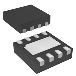
Images are for reference only
X322512MSB4SI
- Manufacturer
- Mfr. Part #X322512MSB4SI
- Package
- Datasheet X322512MSB4SI DataSheet
- In Stock25430
100% Original & New
24 Hours ready to ship
365 Days Warranty
RFQ & Get more Discounts
Specifications
| Manufacturer | YXC Crystal Oscillators |
| Package | SMD3225-4P |
| Operating Temperature | -40℃~+85℃ |
| Frequency | 12MHz |
| Frequency Stability | ±20ppm |
| Normal temperature Frequency Tolerance | ±10ppm |
| Load Capacitance | 20pF |
| Type | Surface Mount Crystal |
Overview
Description
In general, DRAM chips like the X322512MSB4SI are critical for providing temporary storage for data that a computer or device is actively using, allowing for quick access and processing. This type of memory is volatile, meaning it loses its data when power is turned off.
Applications of such DRAM modules include desktops, laptops, servers, and embedded systems, where fast data retrieval and temporary storage are essential for performance. Understanding the specifics of the X322512MSB4SI can help in selecting the appropriate memory for various technological needs.
Features
1. Core Architecture: MIPS M4K core, delivering high-speed processing.
2. Clock Speed: Operates up to 80 MHz.
3. Memory: 512 KB Flash memory and 128 KB SRAM for robust data handling.
4. I/O Ports: Multiple GPIO pins for versatile interfacing options.
5. Peripheral Support: Includes SPI, I2C, UART, ADC, and PWM modules, enabling diverse applications.
6. Integrated Debugging: Supports on-chip debugging tools for easy development.
7. Power Management: Features low-power modes to optimize energy consumption.
8. Operating Voltage: Typically operates at 2.3V to 3.6V.
These attributes make the X322512MSB4SI suitable for a variety of applications, from industrial control to consumer electronics.
Package
Pinout
### Pin Functions:
1. VCC (Pin 1): Power supply.
2. GND (Pin 2): Ground.
3. SDA (Pin 3): Serial Data Line for data transfer.
4. SCL (Pin 4): Serial Clock Line for synchronization.
5. WP (Pin 5): Write Protect; when high, prevents write operations.
6. A0 (Pin 6): Address pin for selecting multiple devices on the same bus.
7. A1 (Pin 7): Address pin for selecting multiple devices on the same bus.
8. NC (Pin 8): No Connect; not connected internally.
This EEPROM is commonly used for applications requiring non-volatile memory storage with a simple serial interface.
Manufacturer
Application
Equivalent
1. CY62167DV30 - Cypress Semiconductor
2. IS62WV5128BLL - Integrated Silicon Solution (ISSI)
3. MT48LC4M16A2 - Micron Technology
4. W631GG6KB - Winbond Electronics
Always verify compatibility in terms of voltage, timing, and pin configuration.
Shipping
Shipping MethodsWe
offer global shipping services through DHL, FedEx, TNT, UPS, or any other forwarder of your choice.
Shipping Fee Reference (DHL/FedEx):
DHL: Shipping cost ranges from $25-$45 (0.5kg), with an estimated delivery time of 2-5 business days.
FedEx: Shipping cost ranges from $25-$40 (0.5kg), with an estimated delivery time of 3-7 business days.
UPS: Shipping cost ranges from $25-$45 (0.5kg), with an estimated delivery time of 3-7 business days.
TNT: Shipping cost ranges from $25-$65 (0.5kg), with an estimated delivery time of 3-7 business days.
EMS: Shipping cost ranges from $30-$50 (0.5kg), with an estimated delivery time of 7-15 business days.
Registered Air Mail: Shipping cost is $2-$4 (0.1kg), with an estimated delivery time of 5-20 business days.
Payments
Payment Methods
The Payment term is 100% Prepaid.
Currently, we only accept the below payment methods:
1. PayPal
2. Credit/ Debit Card
3. Wire Transfer
Similar
-
![MX25R8035FM1IL0]() MX25R8035FM1IL0
MX25R8035FM1IL0
Macronix
-
![MX29F400CBTI-70G]() MX29F400CBTI-70G
MX29F400CBTI-70G
Macronix
-
![MX25R6435FBDIL0]() MX25R6435FBDIL0
MX25R6435FBDIL0
Macronix
-
![MX25U3232FZBI02]() MX25U3232FZBI02
MX25U3232FZBI02
Macronix
-
![MX25L12833FZ2I-10G]() MX25L12833FZ2I-10..
MX25L12833FZ2I-10..
Macronix
-
![MX25L12835FZ2I-10G]() MX25L12835FZ2I-10..
MX25L12835FZ2I-10..
Macronix
-
![MX29F040CQI-70G]() MX29F040CQI-70G
MX29F040CQI-70G
Macronix
-
![MX25L25645GXDI-08G]() MX25L25645GXDI-08..
MX25L25645GXDI-08..
Macronix
-
![MX29F040CTI-70G]() MX29F040CTI-70G
MX29F040CTI-70G
Macronix
-
![MX29LV640ETTI-70G]() MX29LV640ETTI-70G
MX29LV640ETTI-70G
Macronix
-
![MX25L25735FMI-10G]() MX25L25735FMI-10G
MX25L25735FMI-10G
Macronix
-
![MX25U51245GZ4I00]() MX25U51245GZ4I00
MX25U51245GZ4I00
Macronix