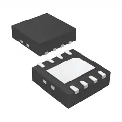
Images are for reference only
XC3S2000-4FGG676C
IC FPGA 489 I/O 676FBGA
- Manufacturer
- Mfr. Part #XC3S2000-4FGG676C
- Package FBGA-676
- Datasheet
- In Stock5451
100% Original & New
24 Hours ready to ship
365 Days Warranty
RFQ & Get more Discounts
Specifications
| Package | Tray |
| Series | Spartan®-3 |
| ProductStatus | Active |
| NumberofLABs/CLBs | 5120 |
| NumberofLogicElements/Cells | 46080 |
| TotalRAMBits | 737280 |
| NumberofI/O | 489 |
| NumberofGates | 2000000 |
| Voltage-Supply | 1.14V ~ 1.26V |
| MountingType | Surface Mount |
| OperatingTemperature | 0°C ~ 85°C (TJ) |
| Package/Case | 676-BGA |
Overview
Description
The "4" in the part number indicates the speed grade, while "FGG" signifies the package type, which is a Fine Pitch Ball Grid Array (FBGA), allowing for a compact design with a high pin count. The XC3S2000 is programmable via standard design tools like Vivado and ISE, making it accessible for developers to implement custom logic. Its versatility, combined with cost-effectiveness and reliability, makes it a popular choice for prototyping and production in industries such as telecommunications, automotive, and consumer electronics.
Features
1. Logic Cells: Approximately 2,000 logic cells, allowing for a variety of digital designs.
2. Configurable I/O: 676 I/O pins with support for various standards including LVTTL, LVCMOS, and PCI.
3. Dynamically Reconfigurable: Supports partial reconfiguration, enabling updates without halting operation.
4. Memory: 128 Kbits of distributed RAM and 4 Mbits of block RAM for data storage.
5. DSP Slices: Integrated DSP slices for efficient digital signal processing tasks.
6. Clock Management: Features global clock networks and phase-locked loops (PLLs) for timing management.
7. Power Consumption: Designed for low power operation, making it suitable for battery-powered applications.
8. Development Tools: Compatible with Xilinx ISE development environment for design and simulation.
Overall, the XC3S2000-4FGG676C is ideal for embedded systems, automotive applications, and other designs requiring flexibility and scalability.
Package
Pinout
The main functions of the XC3S2000 include:
- Implementing digital logic circuits.
- Supporting a variety of I/O standards such as LVTTL, LVCMOS, and others.
- Enabling high-speed serial communication protocols.
- Providing programmable interconnect resources for custom circuit designs.
- Supporting embedded block RAM for data storage.
This FPGA is used in applications such as communications, automotive, industrial control, and consumer electronics, among others, where customization and adaptability are essential.
Manufacturer
Application
Equivalent
Shipping
Shipping MethodsWe
offer global shipping services through DHL, FedEx, TNT, UPS, or any other forwarder of your choice.
Shipping Fee Reference (DHL/FedEx):
DHL: Shipping cost ranges from $25-$45 (0.5kg), with an estimated delivery time of 2-5 business days.
FedEx: Shipping cost ranges from $25-$40 (0.5kg), with an estimated delivery time of 3-7 business days.
UPS: Shipping cost ranges from $25-$45 (0.5kg), with an estimated delivery time of 3-7 business days.
TNT: Shipping cost ranges from $25-$65 (0.5kg), with an estimated delivery time of 3-7 business days.
EMS: Shipping cost ranges from $30-$50 (0.5kg), with an estimated delivery time of 7-15 business days.
Registered Air Mail: Shipping cost is $2-$4 (0.1kg), with an estimated delivery time of 5-20 business days.
Payments
Payment Methods
The Payment term is 100% Prepaid.
Currently, we only accept the below payment methods:
1. PayPal
2. Credit/ Debit Card
3. Wire Transfer
Similar
-
![MX25R8035FM1IL0]() MX25R8035FM1IL0
Macronix
-
![MX25L3233FZBI-08Q]() MX25L3233FZBI-08Q
Macronix
-
![MX25L3233FM1I-08Q]() MX25L3233FM1I-08Q
Macronix
-
![MX25V2033FM1I]() MX25V2033FM1I
Macronix
-
![MX25V16066M1I02]() MX25V16066M1I02
Macronix
-
![MX25R3235FZNIL0]() MX25R3235FZNIL0
Macronix
-
![MX25L8035EM2I-10G]() MX25L8035EM2I-10G
Macronix
-
![MX25U25643GZNI00]() MX25U25643GZNI00
Macronix
-
![MX25U6435FM2I-10G]() MX25U6435FM2I-10G
Macronix
-
![MX25L12833FM2I-10G]() MX25L12833FM2I-10..
Macronix
-
![MX25L12833FZNI-10G]() MX25L12833FZNI-10..
Macronix
-
![MX25L25645GXDI-08G]() MX25L25645GXDI-08..
Macronix