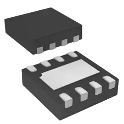
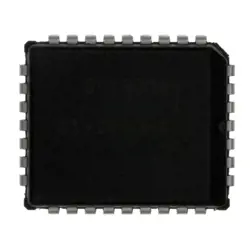
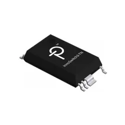
Images are for reference only
XCF16PFS48C
IC PROM SRL 1.8V 16M 48CSBGA
- Manufacturer
- Mfr. Part #XCF16PFS48C
- Package 48-TFBGA
- Datasheet
- In Stock6644
100% Original & New
24 Hours ready to ship
365 Days Warranty
RFQ & Get more Discounts
Specifications
| Package | Tray |
| ProductStatus | Obsolete |
| ProgrammableType | In System Programmable |
| MemorySize | 16Mb |
| Voltage-Supply | 1.65V ~ 2V |
| OperatingTemperature | -40°C ~ 85°C |
| MountingType | Surface Mount |
| Package/Case | 48-TFBGA, CSPBGA |
Overview
Description
The XCF16PFS48C is particularly notable for its dual-boot capability, enabling it to switch between two different configuration files, which can be useful for application updates or recovery. It supports fast read and write operations, making it suitable for high-performance applications. Additionally, the device is designed for robustness, with features like security bits to protect configuration data from unauthorized access.
Overall, the XCF16PFS48C is an essential component for engineers working with Xilinx FPGAs, offering reliability and flexibility in configuration management.
Features
1. Storage Capacity: 16 Megabits, suitable for configuring various Xilinx FPGAs.
2. Interface: Supports a parallel interface, allowing for high-speed data transfer.
3. Voltage Range: Operates at a voltage range of 3.0V to 3.6V, compatible with many digital circuits.
4. Speed: Offers fast access times, enhancing performance in data-intensive applications.
5. Programmability: The device can be reprogrammed multiple times, making it flexible for different design iterations.
6. Package Type: Available in a 48-pin TSOP package, facilitating easy integration into various applications.
7. Endurance: Provides high endurance with the ability to withstand numerous write/erase cycles, ensuring long-lasting performance.
This device is ideal for applications requiring reliable non-volatile storage, such as in communication systems, automotive electronics, and consumer devices.
Package
Pinout
1. Data Interface: Used for data input/output to transfer configuration data.
2. Control Signals: Pins for controlling the device operations, such as initialization and mode selection.
3. Power Supply: Pins for VCC and ground connections.
4. Configuration Mode: Pins for selecting the type of configuration (e.g., JTAG or serial).
5. Status Signals: Pins that provide feedback on the status of the device, such as completion of configuration.
This device enables fast and reliable loading of FPGA configurations, facilitating effective system design and implementation.
Manufacturer
Application
Equivalent
Shipping
Shipping MethodsWe
offer global shipping services through DHL, FedEx, TNT, UPS, or any other forwarder of your choice.
Shipping Fee Reference (DHL/FedEx):
DHL: Shipping cost ranges from $25-$45 (0.5kg), with an estimated delivery time of 2-5 business days.
FedEx: Shipping cost ranges from $25-$40 (0.5kg), with an estimated delivery time of 3-7 business days.
UPS: Shipping cost ranges from $25-$45 (0.5kg), with an estimated delivery time of 3-7 business days.
TNT: Shipping cost ranges from $25-$65 (0.5kg), with an estimated delivery time of 3-7 business days.
EMS: Shipping cost ranges from $30-$50 (0.5kg), with an estimated delivery time of 7-15 business days.
Registered Air Mail: Shipping cost is $2-$4 (0.1kg), with an estimated delivery time of 5-20 business days.
Payments
Payment Methods
The Payment term is 100% Prepaid.
Currently, we only accept the below payment methods:
1. PayPal
2. Credit/ Debit Card
3. Wire Transfer
Similar
-
![MX25R8035FM1IL0]() MX25R8035FM1IL0
MX25R8035FM1IL0
Macronix
-
![MX25V1635FZNQ03]() MX25V1635FZNQ03
MX25V1635FZNQ03
Macronix
-
![MX29GL512FHXFI-11G]() MX29GL512FHXFI-11..
MX29GL512FHXFI-11..
Macronix
-
![MX25L2006EM1I-12G]() MX25L2006EM1I-12G
MX25L2006EM1I-12G
Macronix
-
![MX25R1635FZUIH0]() MX25R1635FZUIH0
MX25R1635FZUIH0
Macronix
-
![MX25U3232FZBI02]() MX25U3232FZBI02
MX25U3232FZBI02
Macronix
-
![MX25L12833FM2I-10G]() MX25L12833FM2I-10..
MX25L12833FM2I-10..
Macronix
-
![MX25L12835FZ2I-10G]() MX25L12835FZ2I-10..
MX25L12835FZ2I-10..
Macronix
-
![MX29F040CQI-70G]() MX29F040CQI-70G
MX29F040CQI-70G
Macronix
-
![MX29LV640ETTI-70G]() MX29LV640ETTI-70G
MX29LV640ETTI-70G
Macronix
-
![MX25U51245GZ4I00]() MX25U51245GZ4I00
MX25U51245GZ4I00
Macronix
-
![MX66U1G45GMI00]() MX66U1G45GMI00
MX66U1G45GMI00
Macronix