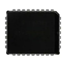
Images are for reference only
SC89171QDNR
- Manufacturer
- Mfr. Part #SC89171QDNR
- Package
- Datasheet
- In Stock14382
100% Original & New
24 Hours ready to ship
365 Days Warranty
RFQ & Get more Discounts
Specifications
| Manufacturer | JLCPCB Assembly |
| Package | QFN-24 (3.5x5.5x0.75) |
Overview
Description
This LDO can supply a specific output current while maintaining regulation under varying load conditions. It often includes protection features such as thermal shutdown and overcurrent protection, ensuring reliability and safety during operation.
The SC89171QDNR is available in a compact package, facilitating space-saving designs in consumer electronics, automotive, and industrial applications. Its performance characteristics, including fast transient response and low noise output, make it ideal for sensitive analog circuits.
For detailed specifications, including electrical characteristics and application circuits, consulting the manufacturer's datasheet is recommended.
Features
1. Input Voltage Range: Supports a wide input voltage range, typically up to 5.5V.
2. Output Voltage: Adjustable output voltage options, providing flexibility for various systems.
3. Low Dropout Voltage: Features low dropout voltage, ensuring stable output even with minimal input-output voltage differential.
4. High Output Current: Capable of delivering significant output current, suitable for powering demanding loads.
5. Low Quiescent Current: Designed for energy efficiency, minimizing power consumption during idle states.
6. Thermal Protection: Includes built-in thermal shutdown to prevent overheating.
7. Short-Circuit Protection: Offers short-circuit protection, enhancing reliability and safety.
8. Compact Package: Available in a small footprint package, ideal for space-constrained applications.
These features make the SC89171QDNR suitable for applications in consumer electronics, automotive, and industrial sectors, where efficient power management is critical.
Package
Pinout
1. Pin 1 (Offset Null): Used for offset voltage adjustment.
2. Pin 2 (Inverting Input, A): Inverting input for the first op-amp.
3. Pin 3 (Non-inverting Input, A): Non-inverting input for the first op-amp.
4. Pin 4 (Output, A): Output for the first op-amp.
5. Pin 5 (Supply Voltage, V- or GND): Negative power supply or ground.
6. Pin 6 (Output, B): Output for the second op-amp.
7. Pin 7 (Non-inverting Input, B): Non-inverting input for the second op-amp.
8. Pin 8 (Inverting Input, B): Inverting input for the second op-amp.
This configuration allows the device to be used in various analog signal processing applications.
Manufacturer
Application
Equivalent
Shipping
Shipping MethodsWe
offer global shipping services through DHL, FedEx, TNT, UPS, or any other forwarder of your choice.
Shipping Fee Reference (DHL/FedEx):
DHL: Shipping cost ranges from $25-$45 (0.5kg), with an estimated delivery time of 2-5 business days.
FedEx: Shipping cost ranges from $25-$40 (0.5kg), with an estimated delivery time of 3-7 business days.
UPS: Shipping cost ranges from $25-$45 (0.5kg), with an estimated delivery time of 3-7 business days.
TNT: Shipping cost ranges from $25-$65 (0.5kg), with an estimated delivery time of 3-7 business days.
EMS: Shipping cost ranges from $30-$50 (0.5kg), with an estimated delivery time of 7-15 business days.
Registered Air Mail: Shipping cost is $2-$4 (0.1kg), with an estimated delivery time of 5-20 business days.
Payments
Payment Methods
The Payment term is 100% Prepaid.
Currently, we only accept the below payment methods:
1. PayPal
2. Credit/ Debit Card
3. Wire Transfer
Similar
-
![MX29F400CBTI-70G]() MX29F400CBTI-70G
MX29F400CBTI-70G
Macronix
-
![MX66U1G45GXDI00]() MX66U1G45GXDI00
MX66U1G45GXDI00
Macronix
-
![MX25V5126FM1I]() MX25V5126FM1I
MX25V5126FM1I
Macronix
-
![MX30LF2G28AD-TI]() MX30LF2G28AD-TI
MX30LF2G28AD-TI
Macronix
-
![MX25L25673GMI-10G]() MX25L25673GMI-10G
MX25L25673GMI-10G
Macronix
-
![MX29GL512FHXFI-11G]() MX29GL512FHXFI-11..
MX29GL512FHXFI-11..
Macronix
-
![MX25U51279GXDR00]() MX25U51279GXDR00
MX25U51279GXDR00
Macronix
-
![MX25U25643GZNI00]() MX25U25643GZNI00
MX25U25643GZNI00
Macronix
-
![MX25U6435FM2I-10G]() MX25U6435FM2I-10G
MX25U6435FM2I-10G
Macronix
-
![MX25L12835FZ2I-10G]() MX25L12835FZ2I-10..
MX25L12835FZ2I-10..
Macronix
-
![MX29F040CQI-70G]() MX29F040CQI-70G
MX29F040CQI-70G
Macronix
-
![MX25L25645GXDI-08G]() MX25L25645GXDI-08..
MX25L25645GXDI-08..
Macronix