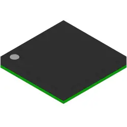
Images are for reference only
XC2S50-5FG256I
IC FPGA 176 I/O 256FBGA
- Manufacturer
- Mfr. Part #XC2S50-5FG256I
- Package BGA256
- Datasheet
- In Stock5482
100% Original & New
24 Hours ready to ship
365 Days Warranty
RFQ & Get more Discounts
Specifications
| Package | Tray |
| Series | Spartan®-II |
| ProductStatus | Active |
| NumberofLABs/CLBs | 384 |
| NumberofLogicElements/Cells | 1728 |
| TotalRAMBits | 32768 |
| NumberofI/O | 176 |
| NumberofGates | 50000 |
| Voltage-Supply | 2.375V ~ 2.625V |
| MountingType | Surface Mount |
| OperatingTemperature | -40°C ~ 100°C (TJ) |
| Package/Case | 256-BGA |
Overview
Description
This FPGA is housed in a 256-pin Fine Pitch Ball Grid Array (FBGA) package, allowing for efficient space utilization in compact designs. The XC2S50-5FG256I supports various I/O standards and offers features like reconfigurability and parallel processing capabilities, making it ideal for applications in telecommunications, automotive, consumer electronics, and industrial control systems.
Key features include low power consumption, built-in multipliers for DSP applications, and support for JTAG programming. It is designed for ease of use with Xilinx’s development tools, facilitating the design and implementation of custom hardware solutions.
Features
- Logic Cells: 50,000 equivalent system gates, providing flexibility for a variety of designs.
- I/O Pins: Up to 192 I/O pins that support various I/O standards, enabling integration with different peripherals.
- Memory: Embedded block RAM (BRAM) for data storage, with a total of 1.4 Mb.
- Speed Grade: -5 indicating a maximum operating frequency of up to 250 MHz.
- Package: Available in a Fine-Pitch Ball Grid Array (FG256) package, allowing for compact designs.
- Configuration: Can be configured through JTAG or serial modes, with options for both single and multi-boot.
- Power Consumption: Low power operation, making it suitable for battery-operated devices.
Overall, the XC2S50-5FG256I is ideal for applications in communications, automotive, industrial control, and consumer electronics requiring moderate complexity with efficiency.
Package
Pinout
Pin Functions:
1. I/O Pins: Used for general input/output operations, supporting various voltage levels and drive strengths.
2. Power Supply Pins: Supply core and I/O voltages, typically +1.5V for core and +3.3V for I/O.
3. Ground Pins: Provide a common return path for electrical current.
4. Configuration Pins: Used to load configuration data into the FPGA, typically through JTAG or other methods.
5. Dedicated Clock Pins: For connecting external clocks.
This FPGA is suitable for applications requiring programmable logic, such as digital signal processing, control systems, and communication interfaces.
Manufacturer
Application
Equivalent
Shipping
Shipping MethodsWe
offer global shipping services through DHL, FedEx, TNT, UPS, or any other forwarder of your choice.
Shipping Fee Reference (DHL/FedEx):
DHL: Shipping cost ranges from $25-$45 (0.5kg), with an estimated delivery time of 2-5 business days.
FedEx: Shipping cost ranges from $25-$40 (0.5kg), with an estimated delivery time of 3-7 business days.
UPS: Shipping cost ranges from $25-$45 (0.5kg), with an estimated delivery time of 3-7 business days.
TNT: Shipping cost ranges from $25-$65 (0.5kg), with an estimated delivery time of 3-7 business days.
EMS: Shipping cost ranges from $30-$50 (0.5kg), with an estimated delivery time of 7-15 business days.
Registered Air Mail: Shipping cost is $2-$4 (0.1kg), with an estimated delivery time of 5-20 business days.
Payments
Payment Methods
The Payment term is 100% Prepaid.
Currently, we only accept the below payment methods:
1. PayPal
2. Credit/ Debit Card
3. Wire Transfer
Similar
-
![MX25V1635FZNI]() MX25V1635FZNI
Macronix
-
![MX25V2033FM1I]() MX25V2033FM1I
Macronix
-
![MX25R3235FZNIL0]() MX25R3235FZNIL0
Macronix
-
![MX30LF2G28AD-TI]() MX30LF2G28AD-TI
Macronix
-
![MX25L8035EM2I-10G]() MX25L8035EM2I-10G
Macronix
-
![MX25L25673GMI-08G]() MX25L25673GMI-08G
Macronix
-
![MX29GL512FHXFI-11G]() MX29GL512FHXFI-11..
Macronix
-
![MX25U25643GZNI00]() MX25U25643GZNI00
Macronix
-
![MX25L2006EM1I-12G]() MX25L2006EM1I-12G
Macronix
-
![MX25V1635FM2I]() MX25V1635FM2I
Macronix
-
![MX25L6433FM2I-08G]() MX25L6433FM2I-08G
Macronix
-
![MX25L12835FZ2I-10G]() MX25L12835FZ2I-10..
Macronix